Trace Resistance Calculator
Trace Resistance Calculator
|
Ω
|
What is a PCB Trace?
A Printed Circuit Board (PCB) is a laminated structure of insulating and conductive layers sandwiched together. PCBs are used for two complementary functions. The first is to mechanically affix electronic components in their designated locations on the outer layers through soldering. The second is to electrically connect the components using tracks, signal traces, or conductive pathways in a controlled manner often known as a PCB design. PCBs are widely employed in the manufacturing of electronic components and appliances.
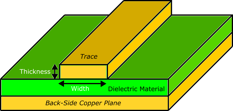
In electronics, a circuit trace or signal trace on an Integrated Circuit(IC) or a Printed Circuit Board (PCB) is comparable to a wire of conducting signals. Each trace is etched from copper sheets laminated onto an insulating (non-conductive) substrate. It thus comprises a flat, narrow portion of the copper sheet that remains after etching. When it comes to PCBs, a trace is a network of printed wiring, copper, fuses, and insulation that make up a Printed Circuit Board, as shown to the right:
As electrical current flows through a trace it generates a considerable amount of heat. PCB traces are manufactured using copper, as it has superior thermal and electrical conductivity. Thus, as current flows along the PCB trace, the copper prevents the heat from stressing and damaging the rest of the PCB structure. On the other hand, the PCB substrate should be made of materials that don’t conduct electrical current, as this would interfere with the electricity pathway as it moves through the printed wires. In fact, dielectric materials make up the PCB insulation that functions as the laminated electrical insulator of the PCB circuitry.
Like electrical current, a trace is an essential part of nearly every circuit board. If it is not designed correctly, it can cause errors in the circuitry of electronic devices which may take a lot of time and resources to fix. Similarly, PCBs have many components, it’s thus very essential that you exactly know which parts and materials are required to assemble or repair a Printed Circuit Board. In this article, we’ll focus on calculating the resistance of a PCB trace.
What is Trace Resistance?
In an electric circuit, resistance is the measure of opposition to charge flow (current flow). Its units of measurement are ohms, and it’s symbolized by Ω -a Greek letter omega. Naturally, each and every material existing in the universe has some amount of resistance to current flow alongside other properties. For this reason, all materials are broadly categorized as conductors-with negligible resistance or insulators with very high resistance. Although copper is the most commonly used material in PCB traces, it comes with different properties and compositions. Thus, despite being made of copper (a very good electrical conductor) PCB traces still have some opposition to current flow; which is referred to as PCB trace resistance.
PCB trace resistance is determined by the thickness, width, and length of the trace. It is one of the most crucial factors that should be calculated and analyzed when designing a PCB. This is because the value of the trace resistance may lead to various design modifications and implementation issues. And as the PCB circuit complexity increases, the implementation issues are bound to increase as well. Moreover, the trace resistance value must be sufficiently low for current to flow through the PCB circuitry.
Why is it Important to Calculate Trace Resistance?
From Ohm’s law, resistance is expressed as: ? = ? / ?, where R is the overall Resistance, V is the circuit Voltage, and I is the current in the circuit. The expression shows that resistance is inversely proportional to the current in the circuit. That means, the lower the resistance, the higher the amount of current flow and vice versa.
On the other hand, electrical current is directly proportional to power according to: ? = ??. Where P is output/input power, V has applied voltage and I is circuit current. Thus, trace resistance is an important factor when determining the power consumption of any electronic system consisting of Integrated Circuits or Printed Circuit Boards. Similarly, by calculating the trace resistance, you can evaluate the amount of power that can be dissipated by the PCB trace itself.
In addition, the current that flows through the copper PCB traces generate a considerable amount of heat. And as previously stated, trace resistance is a function of the thickness, length, and width of a PCB trace. Thus, if these dimensions are correctly calibrated, especially width and thickness, they can help minimize the buildup of heat. As we will see later from the PCB trace resistance equation; the wider the PCB trace, the lower its resistance to current flow, and in such a case, heat build-up will much lesser. Lastly, trace resistance calculation is very important, as it allows you to evaluate the contribution of a PCB trace to the overall circuit resistance.
An example of a real-life application of Trace Resistance calculations is in Microstrips. Microstrips are electronic devices popularly used in Microwave Radio Frequency (RF) technologies. Often, you’ll come across Microstrip antennas in satellites, aircraft, missiles, mobile phones, radars, wireless communication systems, and remote sensing. They were invented to counter the physical limitations of manufacturing capacitors and inductors for use at such very high frequencies.
A Microstrip is made out of printed circuit boards (PCBs) whose dimensions are carefully calibrated to meet specific parameters. One such parameter is trace resistance. By calculating its trace resistance, you can evaluate how much power the Microstrip dissipates as well as its contribution to overall circuit resistance in an RF system.
How do you Calculate Trace Resistance?
A specific formula is used to calculate PCB trace resistance, it is expressed as:
? = ? × [? / (? × ? )] ×[1 + ? × (????−25℃)]………(?)
Where:
? = Trace Resistance
? = Resistivity of (PCB trace material) Copper at 20℃, which is 1.7 ×10⁻⁶ Ω .cm (ohm-centimetre)
? = Trace Length, or the end-to-end distance of the PCB trace

? = Trace Width, which can be obtained using a PCB trace width Calculator
? = Trace Thickness, it can be thought as the Trace Height
? = Temperature Coefficient of Copper at 20℃, which is 0.393% ??? ℃ or 3.9 × 10⁻³ [1℃]
???? = Ambient Temperature[℃] of the environment in which the PCB trace is operating
As shown in the figure to the right, the Trace Thickness (T) is the vertical dimension of a PCB trace whereas Trace Width (W) is the horizontal measurement of the trace.
Note: The temperature coefficient of Copper +0.393% ??? ℃, is given at near room temperature. This means that if the temperature of the PCB trace were to increase by 1℃, then the trace resistance will increase by 0.393%. Also, the trace resistance formula in eqn. (i) can only be used to determine a close enough approximate value of PCB trace resistance. As the physical trace resistance is bound to vary slightly after production.
Examples of PCB Trace Resistance Calculations
Calculating the resistance of a PCB trace using equation (i), is as simple as applying the ohms law with known parameters. Here are some examples:
Example 1: Calculate the resistance of a PCB trace given the following parameters: Length (L) = 2 inch, Trace height (T) = 3mm, Width (W) = 2mm, Ambient Temperature (????Tamb) = 37.5 °C.
Solution: Given that,
? = 1.7 × 10⁻⁸ Ω .m (ohm-meter)
? = 2 ?? = 2 × 0.0254 = 0.0508 ?
? = 2 ?? = 2 × 10⁻³ ?
T= 3 ?? = 3 × 10⁻³ ?
? = 3.9 × 10⁻³ [1℃]
???? = 37.5 ℃
We’ll use the following formula,
? = ? × [? / (? × ?)] × [1 + ? × (???? − 25℃)]………(?)
Substituting the above parameters in eq. (i) we get:
? = ? × [? / (? × ?)] × [1 + ? × (???? − 25℃)]………(?)
? = (1.7 ×10⁻⁸ Ω .m ) × [ 0.0508? / (2 × 10⁻³ ? × 3 × 10⁻³ ?) ] × [1 + 3.9 × 10−3 × (37.5 − 25)]
? = 1.5094 × 10⁻⁴ Ω
Hence, the Trace Resistance will be: ? ≈ 0.000151 Ω
Example 2: Considering the following parameters: Length (L) = 10.5 inch, Trace height (T) = 1.57mm, Width = 4.6 mil, Ambient Temperature (????) = 30 °C. Determine the trace resistance?
Solution:
The parameters to be used in solving this problem are:
? = 1.7 × 10⁻⁶ Ω cm (ohm-centimeter)
? = 10.5 ?? = 10.5 × 2.54 = 26.67 ??
? = 4.6 ??? = 4.6 × 0.00254 ?? = 0.011684 ??
? = 1.57mm = 1.57 × 10⁻¹ ??
? = 3.9 × 10⁻³ [1℃] ???? = 30 ℃
The formula for trace resistance is:
? = ? × [? / (? × ?)] × [1 + ? × (???? − 25 ℃)]
Let’s substitute the given parameter values in the formula above:
? = 1.7 × 10⁻⁶ Ω cm × [26.67 ?? / (0.011684 ?? × (1.57 × 10⁻¹ ??))] × [1 + (3.9 × 10⁻³ [1℃]) × (30 ℃ − 25℃)]
? = 0.02519
Hence, the Trace Resistance will be:
? ≈ 0.0252 Ω
Note: When calculating Trace Resistance manually (by hand computations), you should convert the units of the physical dimensions of the PCB trace (Length, Width, and Thickness) into either centimeter (cm) or meters (m). This is because, the Resistivity of copper at 20℃ is commonly given as: 1.7 ×10⁻⁶ Ω cm or 1.7 ×10⁻⁸ Ω m; and we need the metric units in eq. (i) to cancel out so that we can compute the value of trace resistance in ohms (Ω). Also, the Ambient Temperature (????) should be converted to [°C], for the units to cancel out as well.
How to use a Trace Resistance Calculator
A Trace Resistance Calculator is a tool designed to calculate the resistance of a PCB trace that is made of copper. Its operation is based on the standard formula for calculating trace resistance:
? = ? × [? / (? × ?)] × [1 + ? × (????−25℃)]
The trace resistance calculator works in a very straightforward way: all you need to do is specify the values and units of measurements for the input fields that include the ambient temperature and trace dimensions (Length, Width and Thickness). And on clicking the “Calculate” button you will get the output as the PCB trace resistance in ohms (Ω).
Note: The calculator uses the Resistivity (?) and Temperature Coefficient (?) of Copper at 20℃.
Example: Using a Trace Resistance Calculator, determine the resistance of a PCB trace given the following:
Trace Length (?) = 5 ???ℎ
Trace Width (?) = 4 ???
Trace Thickness (?) = 3 ?? /??2
Ambient Temperature[Equation]) = 38 ℃
Solution: Fill in the calculator’s input fields with the parameter values given above and click “Calculate”, as shown below:
The resulting Trace Resistance value of that PCB trace is:
? ≈ 0.213 Ω
Note: Whenever you’re using the Trace Resistance Calculator you’re not required to perform any unit conversions of the provided PCB trace dimensions and ambient temperature. Also, some trace resistance calculators available online can function in reverse to assist you to determine missing parameters. In such a case, all you’ll need to do is to input enough parameters and the missing value will be calculated automatically.
Most PCB manufacturers have integrated Trace Resistance Calculators in their design suits and development environments, to assist in estimating the resistance of copper traces on the final PCB boards by providing the required dimensions and manufacturing profiles. Such calculators use the standard formula of calculating trace resistance, so they are constant universally. In addition, trace resistance calculators can be applied in determining the resistance of bus bars.
Effects of Trace Resistance
Power Loss: A significant amount of trace resistance is primarily associated with power loss. But small signals on PCBs usually have a negligible effect on the resistance of a PCB trace. On the other hand, power circuits have a significant impact on PCB trace resistance even for the slightest variations in the circuitry parameters. This is because power loss eventually leads to a temperature rise that causes a significant increase in trace resistance, which lowers the conductivity of the circuit.
Interference: In power circuits, the uncompensated resistance of the PCBs trace could act as a fuse causing a power surge and if the PCB trace is burnt, then the damage left will be permanent. While in high-speed digital boards, the resistance and parasitic capacitance of a PCB trace are likely to create oscillations that cause Electromagnetic Interference (EMI) to the overall circuitry.
How to Counter Trace Resistance Effects
As previously stated, trace resistance is a key factor that should be considered in the design stage of a printed circuit board. This means that the most effective way to compensate for the presence of trace resistance is by optimizing the design of a PCB trace. This is achieved by increasing the PCB trace area. For example, you can configure your design tools to layout PCB traces that have sufficient width to avoid a high amount of trace resistance.
For power circuits, you can use additional methods like solder brides to reduce power losses and increase current capacity, other than just using complete PCBs trace. High-speed circuits should be fitted with matched lines to cancel out potential EMI that may be associated with oscillations created by PCB trace resistance. Moreover, sensitive circuits should have sub-circuits to eliminate the impact of PCB trace resistance.
DO Supply Inc. makes no representations as to the completeness, validity, correctness, suitability, or accuracy of any information on this website and will not be liable for any delays, omissions, or errors in this information or any losses, injuries, or damages arising from its display or use. All the information on this website is provided on an "as-is" basis. It is the reader's responsibility to verify their own facts.